BTN.com staff, November 20, 2015
Throughout history, the natural world has inspired important scientific breakthroughs. For example, the Wright brothers incorporated the concepts of lift and drag into airplane designs after they observed how birds in flight tilted their wings back and forth.
At the University of Wisconsin, another pair borrowed from Mother Nature to develop a significant advancement in photographic technology. Their inspiration? The sophisticated eye structure of mammals.
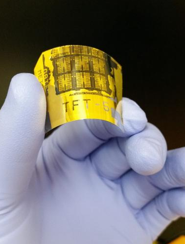
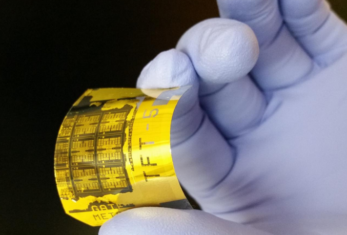
 The University of Wisconsin?s Zhenqiang ?Jack? Ma and research scientist Jung-Hun Seo recently created the thinnest and most flexible phototransistor yet made. They based this innovative technology on the way our eyes organically process images.
?We want to focus the light and image through lenses,? Ma explained. ?So the lens has a curved shape, and the curved shape will form a curved image.?
The main reason photography generally doesn?t render images as well as our own eyesight is that current phototransistors are too firm and rigid.
There are a few exceptions, as Ma pointed out. Some top-of-the-line cameras employ multiple lenses to get a more thorough, dynamic image. There?s just one problem: Most of those cameras also cost tens or even hundreds of thousands of dollars.
Ma?s goal was to make something that most people could use in their daily lives. By making phototransistors that can bend, Ma and his partner hope to make myriad electronic devices, well, picture-perfect.
?Today, where the camera is most used is in the cell phone,? he added. ?I have some digital cameras that are smaller, but we don?t use them anymore because the cell-phone pixels right now are getting bigger and bigger, and you don?t need to carry another digital camera.?
While there are plenty of things that set their technology apart from what?s already on the market, one of the most notable differences is its use of thin silicon. Other scientists use materials like polymer, but Ma said those images are usually quite slow.
?We peel off our silicon very thin,? Ma said. ?It?s about 250 nanometers ? Compared to the materials other people use like polymer, 2-D materials and 1-D materials our materials are much, much faster. If you compare with organic materials ours is 2,000 times faster.?
[btn-post-package]This tremendous advantage is in part due to the duo?s pioneering ?flip-transfer? method of fabrication, which exposes the bottom side of the membrane entirely to light and helps the very thin material work better as a reflector.
This technique, along with other innovations, makes his phototransistor a true standout.
?From the performance [standpoint], ours is the best,? he said. ?From the material used, it?s the least.?
By Grant Rindner


 See what's coming up live on B1G+ every day of the season at BigTenPlus.com.